2. Introduction to Lithography
2.1. Pattern Transfer
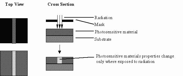
Lithography in the MEMS context is typically the transfer of a pattern to a photosensitive material by selective exposure to a radiation source such as light. A photosensitive material is a material that experiences a change in its physical properties when exposed to a radiation source. If we selectively expose a photosensitive material to radiation (e.g. by masking some of the radiation) the pattern of the radiation on the material is transferred to the material exposed, as the properties of the exposed and unexposed regions differs (as shown in figure 1).

Fig. 1. Transfer of a pattern to a photosensitive material
This discussion will focus on optical lithography, which is simply lithography using a radiation source with wavelength(s) in the visible and near visible spectrums.
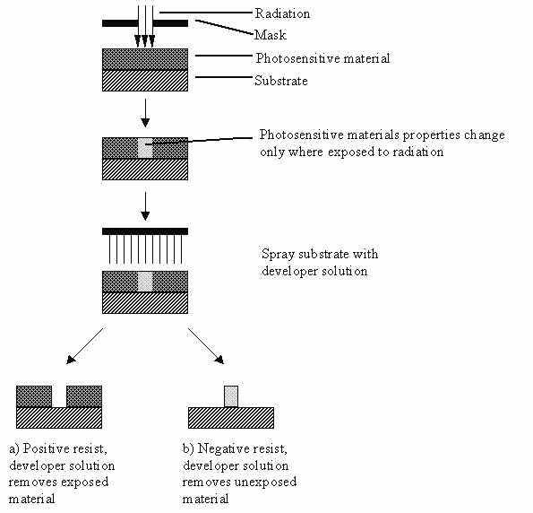
In lithography for micromachining, the photosensitive material used is typically a photoresist (also called resist, other photosensitive polymers are also used). When resist is exposed to a radiation source of a specific a wavelength, the chemical resistance of the resist to developer solution changes. If the resist is placed in a developer solution after selective exposure to a light source, it will etch away one of the two regions (exposed or unexposed). If the exposed material is etched away by the developer and the unexposed region is resilient, the material is considered to be a positive resist (shown in figure 2a). If the exposed material is resilient to the developer and the unexposed region is etched away, it is considered to be a negative resist (shown in figure 2b).

Fig. 2. a) Pattern definition in positive resist, b) Pattern definition in negative resist
Lithography is the principal mechanism for pattern definition in micromachining. Photosensitive compounds are primarily organic, and do not encompass the spectrum of materials properties of interest to micro-machinists. However, as the technique is capable of producing fine features in an economic fashion, a photosensitive layer is often used as a temporary mask when etching an underlying layer, so that the pattern may be transferred to the underlying layer (shown in figure 3a). Photoresist may also be used as a template for patterning material deposited after lithography (shown in figure 3b). The resist is subsequently etched away, and the material deposited on the resist is "lifted off". The deposition template (lift-off) approach for transferring a pattern from resist to another layer is less common than using the resist pattern as an etch mask. The reason for this is that resist is incompatible with many MEMS deposition processes, usually because it cannot withstand high temperatures and may act as a source of contamination.
