Guide
- Deposition
- Lithography
- Etching
One of the basic building blocks in MEMS processing is the ability to deposit thin films of material. In this text we assume a thin film to have a thickness anywhere between a few nanometer to about 100 micrometer. The film can subsequently be locally etched using processes described in the Lithography and Etching sections of this guide.
MEMS deposition technology can be classified in two groups:
These processes exploit the creation of solid materials directly from chemical reactions in gas and/or liquid compositions or with the substrate material. The solid material is usually not the only product formed by the reaction. Byproducts can include gases, liquids and even other solids.
Common for all these processes are that the material deposited is physically moved on to the substrate. In other words, there is no chemical reaction which forms the material on the substrate. This is not completely correct for casting processes, though it is more convenient to think of them that way.
This is by no means an exhaustive list since technologies evolve continuously.
In this process, the substrate is placed inside a reactor to which a number of gases are supplied. The fundamental principle of the process is that a chemical reaction takes place between the source gases. The product of that reaction is a solid material with condenses on all surfaces inside the reactor.
The two most important CVD technologies in MEMS are the Low Pressure CVD (LPCVD) and Plasma Enhanced CVD (PECVD). The LPCVD process produces layers with excellent uniformity of thickness and material characteristics. The main problems with the process are the high deposition temperature (higher than 600°C) and the relatively slow deposition rate. The PECVD process can operate at lower temperatures (down to 300° C) thanks to the extra energy supplied to the gas molecules by the plasma in the reactor. However, the quality of the films tend to be inferior to processes running at higher temperatures. Secondly, most PECVD deposition systems can only deposit the material on one side of the wafers on 1 to 4 wafers at a time. LPCVD systems deposit films on both sides of at least 25 wafers at a time. A schematic diagram of a typical LPCVD reactor is shown in the figure below.
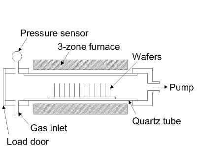
Figure 1: Typical hot-wall LPCVD reactor.
CVD processes are ideal to use when you want a thin film with good step coverage. A variety of materials can be deposited with this technology, however, some of them are less popular with fabs because of hazardous byproducts formed during processing. The quality of the material varies from process to process, however a good rule of thumb is that higher process temperature yields a material with higher quality and less defects.
This process is also known as "electroplating" and is typically restricted to electrically conductive materials. There are basically two technologies for plating: Electroplating and Electroless plating. In the electroplating process the substrate is placed in a liquid solution (electrolyte). When an electrical potential is applied between a conducting area on the substrate and a counter electrode (usually platinum) in the liquid, a chemical redox process takes place resulting in the formation of a layer of material on the substrate and usually some gas generation at the counter electrode.
In the electroless plating process a more complex chemical solution is used, in which deposition happens spontaneously on any surface which forms a sufficiently high electrochemical potential with the solution. This process is desirable since it does not require any external electrical potential and contact to the substrate during processing. Unfortunately, it is also more difficult to control with regards to film thickness and uniformity. A schematic diagram of a typical setup for electroplating is shown in the figure below.
The electrodeposition process is well suited to make films of metals such as copper, gold and nickel. The films can be made in any thickness from ~1µm to >100µm. The deposition is best controlled when used with an external electrical potential, however, it requires electrical contact to the substrate when immersed in the liquid bath. In any process, the surface of the substrate must have an electrically conducting coating before the deposition can be done.
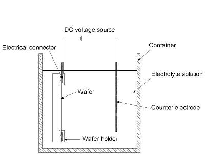
Figure 2: Typical setup for electrodeposition.
This technology is quite similar to what happens in CVD processes, however, if the substrate is an ordered semiconductor crystal (i.e. silicon, gallium arsenide), it is possible with this process to continue building on the substrate with the same crystallographic orientation with the substrate acting as a seed for the deposition. If an amorphous/polycrystalline substrate surface is used, the film will also be amorphous or polycrystalline.
There are several technologies for creating the conditions inside a reactor needed to support epitaxial growth, of which the most important is Vapor Phase Epitaxy (VPE). In this process, a number of gases are introduced in an induction heated reactor where only the substrate is heated. The temperature of the substrate typically must be at least 50% of the melting point of the material to be deposited.
An advantage of epitaxy is the high growth rate of material, which allows the formation of films with considerable thickness (>100µm). Epitaxy is a widely used technology for producing silicon on insulator (SOI) substrates. The technology is primarily used for deposition of silicon. A schematic diagram of a typical vapor phase epitaxial reactor is shown in the figure below.
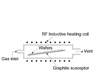
Figure 3: Typical cold-wall vapor phase epitaxial reactor.
This has been and continues to be an emerging process technology in MEMS. The process can be used to form films of silicon with thicknesses of ~1µm to >100µm. Some processes require high temperature exposure of the substrate, whereas others do not require significant heating of the substrate. Some processes can even be used to perform selective deposition, depending on the surface of the substrate.
This is one of the most basic deposition technologies. It is simply oxidation of the substrate surface in an oxygen rich atmosphere. The temperature is raised to 800° C-1100° C to speed up the process. This is also the only deposition technology which actually consumes some of the substrate as it proceeds. The growth of the film is spurned by diffusion of oxygen into the substrate, which means the film growth is actually downwards into the substrate. As the thickness of the oxidized layer increases, the diffusion of oxygen to the substrate becomes more difficult leading to a parabolic relationship between film thickness and oxidation time for films thicker than ~100nm. This process is naturally limited to materials that can be oxidized, and it can only form films that are oxides of that material. This is the classical process used to form silicon dioxide on a silicon substrate. A schematic diagram of a typical wafer oxidation furnace is shown in the figure below.
Whenever you can! This is a simple process, which unfortunately produces films with somewhat limited use in MEMS components. It is typically used to form films that are used for electrical insulation or that are used for other process purposes later in a process sequence.
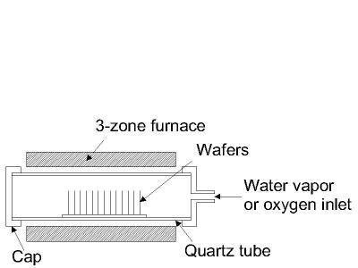
Figure 4: Typical wafer oxidation furnace.
PVD covers a number of deposition technologies in which material is released from a source and transferred to the substrate. The two most important technologies are evaporation and sputtering.
PVD comprises the standard technologies for deposition of metals. It is far more common than CVD for metals since it can be performed at lower process risk and cheaper in regards to materials cost. The quality of the films are inferior to CVD, which for metals means higher resistivity and for insulators more defects and traps. The step coverage is also not as good as CVD.
The choice of deposition method (i.e. evaporation vs. sputtering) may in many cases be arbitrary, and may depend more on what technology is available for the specific material at the time.
In evaporation the substrate is placed inside a vacuum chamber, in which a block (source) of the material to be deposited is also located. The source material is then heated to the point where it starts to boil and evaporate. The vacuum is required to allow the molecules to evaporate freely in the chamber, and they subsequently condense on all surfaces. This principle is the same for all evaporation technologies, only the method used to the heat (evaporate) the source material differs. There are two popular evaporation technologies, which are e-beam evaporation and resistive evaporation each referring to the heating method. In e-beam evaporation, an electron beam is aimed at the source material causing local heating and evaporation. In resistive evaporation, a tungsten boat, containing the source material, is heated electrically with a high current to make the material evaporate. Many materials are restrictive in terms of what evaporation method can be used (i.e. aluminum is quite difficult to evaporate using resistive heating), which typically relates to the phase transition properties of that material. A schematic diagram of a typical system for e-beam evaporation is shown in the figure below.
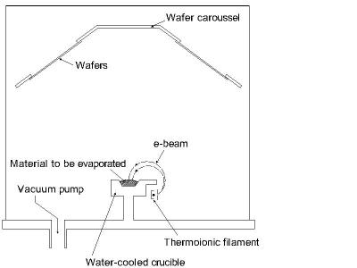
Figure 5: Typical system for e-beam evaporation of materials.
Sputtering is a technology in which the material is released from the source at much lower temperature than evaporation. The substrate is placed in a vacuum chamber with the source material, named a target, and an inert gas (such as argon) is introduced at low pressure. A gas plasma is struck using an RF power source, causing the gas to become ionized. The ions are accelerated towards the surface of the target, causing atoms of the source material to break off from the target in vapor form and condense on all surfaces including the substrate. As for evaporation, the basic principle of sputtering is the same for all sputtering technologies. The differences typically relate to the manor in which the ion bombardment of the target is realized. A schematic diagram of a typical RF sputtering system is shown in the figure below.
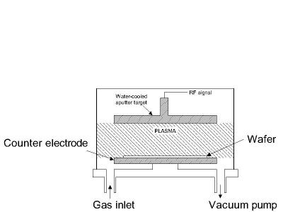
Figure 6: Typical RF sputtering system.
In this process the material to be deposited is dissolved in liquid form in a solvent. The material can be applied to the substrate by spraying or spinning. Once the solvent is evaporated, a thin film of the material remains on the substrate. This is particularly useful for polymer materials, which may be easily dissolved in organic solvents, and it is the common method used to apply photoresist to substrates (in photolithography). The thicknesses that can be cast on a substrate range all the way from a single monolayer of molecules (adhesion promotion) to tens of micrometers. In recent years, the casting technology has also been applied to form films of glass materials on substrates. The spin casting process is illustrated in the figure below.
Casting is a simple technology which can be used for a variety of materials (mostly polymers). The control on film thickness depends on exact conditions, but can be sustained within +/-10% in a wide range. If you are planning to use photolithography you will be using casting, which is an integral part of that technology. There are also other interesting materials such as polyimide and spin-on glass which can be applied by casting.
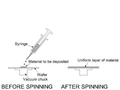
Figure 7: The spin casting process as used for photoresist in photolithography.