Guide
- Deposition
- Lithography
- Etching
In order to form a functional MEMS structure on a substrate, it is necessary to etch the thin films previously deposited and/or the substrate itself. In general, there are two classes of etching processes:
In the following, we will briefly discuss the most popular technologies for wet and dry etching.
This is the simplest etching technology. All it requires is a container with a liquid solution that will dissolve the material in question. Unfortunately, there are complications since usually a mask is desired to selectively etch the material. One must find a mask that will not dissolve or at least etches much slower than the material to be patterned. Secondly, some single crystal materials, such as silicon, exhibit anisotropic etching in certain chemicals. Anisotropic etching in contrast to isotropic etching means different etch rates in different directions in the material. The classic example of this is the <111> crystal plane sidewalls that appear when etching a hole in a <100> silicon wafer in a chemical such as potassium hydroxide (KOH). The result is a pyramid shaped hole instead of a hole with rounded sidewalls with a isotropic etchant. The principle of anisotropic and isotropic wet etching is illustrated in the figure below.
This is a simple technology, which will give good results if you can find the combination of etchant and mask material to suit your application. Wet etching works very well for etching thin films on substrates, and can also be used to etch the substrate itself. The problem with substrate etching is that isotropic processes will cause undercutting of the mask layer by the same distance as the etch depth. Anisotropic processes allow the etching to stop on certain crystal planes in the substrate, but still results in a loss of space, since these planes cannot be vertical to the surface when etching holes or cavities. If this is a limitation for you, you should consider dry etching of the substrate instead. However, keep in mind that the cost per wafer will be 1-2 orders of magnitude higher to perform the dry etching
If you are making very small features in thin films (comparable to the film thickness), you may also encounter problems with isotropic wet etching, since the undercutting will be at least equal to the film thickness. With dry etching it is possible etch almost straight down without undercutting, which provides much higher resolution.
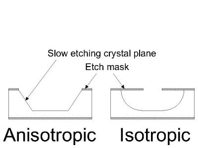
Figure 1: Difference between anisotropic and isotropic wet etching.
The dry etching technology can split in three separate classes called reactive ion etching (RIE), sputter etching, and vapor phase etching.
In RIE, the substrate is placed inside a reactor in which several gases are introduced. A plasma is struck in the gas mixture using an RF power source, breaking the gas molecules into ions. The ions are accelerated towards, and reacts at, the surface of the material being etched, forming another gaseous material. This is known as the chemical part of reactive ion etching. There is also a physical part which is similar in nature to the sputtering deposition process. If the ions have high enough energy, they can knock atoms out of the material to be etched without a chemical reaction. It is a very complex task to develop dry etch processes that balance chemical and physical etching, since there are many parameters to adjust. By changing the balance it is possible to influence the anisotropy of the etching, since the chemical part is isotropic and the physical part highly anisotropic the combination can form sidewalls that have shapes from rounded to vertical. A schematic of a typical reactive ion etching system is shown in the figure below.
A special subclass of RIE which continues to grow rapidly in popularity is deep RIE (DRIE). In this process, etch depths of hundreds of microns can be achieved with almost vertical sidewalls. The primary technology is based on the so-called "Bosch process", named after the German company Robert Bosch which filed the original patent, where two different gas compositions are alternated in the reactor. The first gas composition creates a polymer on the surface of the substrate, and the second gas composition etches the substrate. The polymer is immediately sputtered away by the physical part of the etching, but only on the horizontal surfaces and not the sidewalls. Since the polymer only dissolves very slowly in the chemical part of the etching, it builds up on the sidewalls and protects them from etching. As a result, etching aspect ratios of 50 to 1 can be achieved. The process can easily be used to etch completely through a silicon substrate, and etch rates are 3-4 times higher than wet etching.
Sputter etching is essentially RIE without reactive ions. The systems used are very similar in principle to sputtering deposition systems. The big difference is that substrate is now subjected to the ion bombardment instead of the material target used in sputter deposition.
Vapor phase etching is another dry etching method, which can be done with simpler equipment than what RIE requires. In this process the wafer to be etched is placed inside a chamber, in which one or more gases are introduced. The material to be etched is dissolved at the surface in a chemical reaction with the gas molecules. The two most common vapor phase etching technologies are silicon dioxide etching using hydrogen fluoride (HF) and silicon etching using xenon diflouride (XeF2), both of which are isotropic in nature. Usually, care must be taken in the design of a vapor phase process to not have bi-products form in the chemical reaction that condense on the surface and interfere with the etching process.
The first thing you should note about this technology is that it is expensive to run compared to wet etching. If you are concerned with feature resolution in thin film structures or you need vertical sidewalls for deep etchings in the substrate, you have to consider dry etching. If you are concerned about the price of your process and device, you may want to minimize the use of dry etching. The IC industry has long since adopted dry etching to achieve small features, but in many cases feature size is not as critical in MEMS. Dry etching is an enabling technology, which comes at a sometimes high cost.
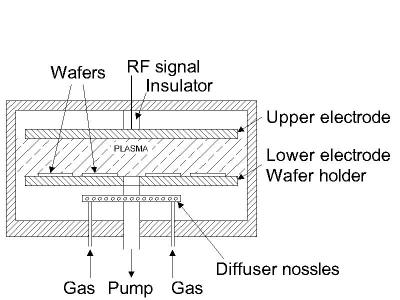
Figure 2: Typical parallel-plate reactive ion etching system.